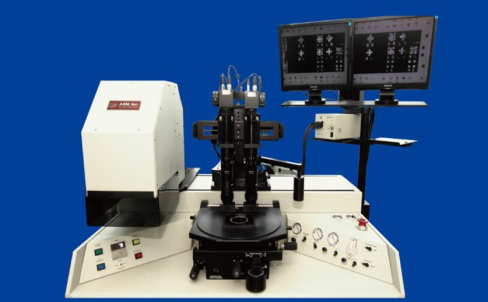
ABM lithography machine can integrate nano-imprint lithography function, template material: Silicon, quartz, nickel and so on, suitable for all kinds of nano-imprint lithography template; Imprint templates can be widely used in renewable energy, microfluidics, nanofluids, light-emitting diodes and lasers, life sciences, such as laboratory on a chip systems, optics, radio frequency components, data storage, semiconductors and other fields.
Main technical parameters:
Beam Uniformity:
---<±1% over 2”zone
---<±2% over 4”zone
---<±3% over 6”zone
Contact exposure characteristic dimensions, CD(near ultraviolet NUV): 0.5 um
Contact exposure characteristic dimensions, CD(deep ultraviolet DUV): 0.35 um
Support proximity exposure,characteristic dimension CD:
- 0.8 um hard contact
- 1 um20um spacing
-2um50umspacing
Frontalignment accuracy ±0.5um
Reverse alignment accuracy ±2-±3um (Depends on user)
Supportpositive photoresist,negativephotoresist,Su8and otherthick gumforlithography. Characteristic dimension:100um-300um
SupportLED excellent current control technology PSStechnology forlithography
Support vacuum, proximity andcontact exposure
Supports constant light intensity or constant power mode